Thin Film Ceramic Substrates

Quality Beo Ceramic Materials Si3n4 Ceramic Manufacturer Ceramic Materials Ceramics Advanced Ceramics
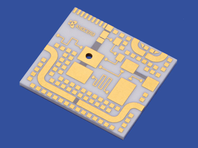
Thin Film Metallized Substrates Products Maruwa Co Ltd

Thin Film Substrates For Microelectronics Coorstek Technical Ceramics
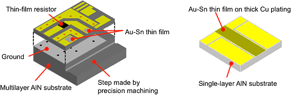
Thin Film Substrates Fine Ceramics Advanced Ceramics Kyocera
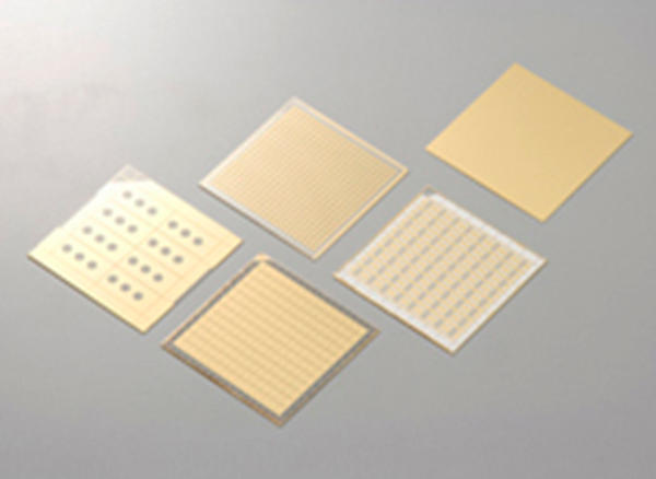
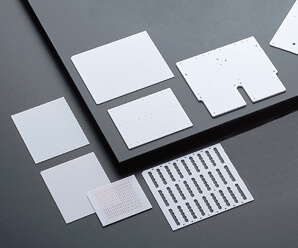
Thin Film Mic Substrates Components For Wireless Communication Devices Ceramic Packages Products Kyocera

Tape Casting Of High Dielectric Ceramic Substrates Google Search It Cast Substrate Tape

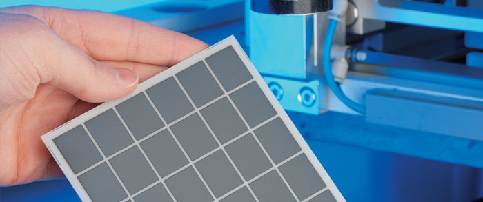
Mpt is a one stop shop for your thick film substrate needs.
Thin film ceramic substrates.

Quality Beo Ceramic Materials Si3n4 Ceramic Manufacturer Ceramic Materials Structural Analysis Material Specification
Pin By Ferrotec Nord On Ferrotec Nord Thin Film Film To Focus
Ceramic Substrates Electronic Circuit Carriers And Circuit Boards Made From Advanced Ceramics

Dpc Substrate Thin Film Supply Better Thermal Management And Smaller Dpc Substrate

Sputtering Process Physical Vapor Deposition Vapor Technology

How To Fabricate A Thin Film Composite Membranes By Electrospinning Nanofibers Technology In 2020 Innovation Centre Membrane Material

Pin On Innovacera Ceramic News
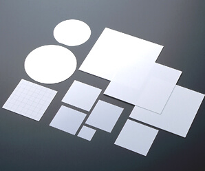
Thick Film Substrates Fine Ceramics Advanced Ceramics Kyocera

Nanodiamond Coating Nanodiamond For Electronics Chemical Vapor Deposition Vapor Chemical
Submounts And Subcarriers Components For Fiber Optic Communication Modules Ceramic Packages Products Kyocera
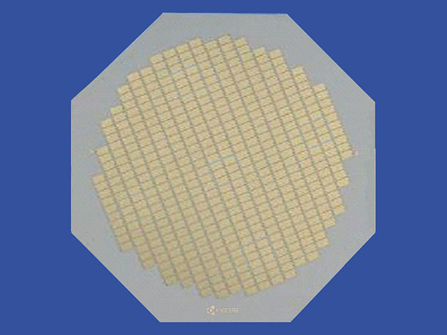
Ceramic Substrates For Probe Cards Ceramic Packages Products Kyocera

Basic Electronics On The Go 14 Fixed Resistors Thick Film And Thin Resistors Basic Electronics

Pin On Crystal Substrates

Quality Beo Ceramic Materials Si3n4 Ceramic Manufacturer Ceramic Materials Advanced Ceramics Properties Of Materials

Aln Crystal Semiconductor Semiconductor Materials Crystal Growth

Thin Film Components And Integration The Next Step In Volumetric Efficiency Inductors Integrity New Product Introduction

Ceramic Substrate An Overview Sciencedirect Topics

Boron Nitride Substrate Heater For Vacuum Deposition Chemical Vapor Deposition Thin Film Ceiling Lights

Quality Beo Ceramic Materials Si3n4 Ceramic Manufacturer Ceramic Materials Advanced Ceramics Properties Of Materials

Thin Film Components And Integration The Next Step In Volumetric Efficiency Disruptive Technology Inductors Integrity

Lead Sulfid Crystal Substrates In 2020 Substrate Crystals Molar Mass

Quality Beo Ceramic Materials Si3n4 Ceramic Manufacturer Ceramic Materials Advanced Ceramics Ceramics

Photo Gallery Furnace Home Decor Copper Foil

Get The Reliable Quality Of Inconel Substrate Heater For Reactive Deposition By The Best Company Substrate Good Things Heater
Source : pinterest.com
